There are two General Purpose I/O (GPIO) Ports, each made of 32 bidirectional pins on the JP1 and JP2 40-pin expansion headers (hence the ports are each 32-bits wide). These ports can be used with some of the lab's peripherals such as the hexkeypad and Lego controller.
| Device | GPIO Port on JP1 & JP2 (can be used with hexkeypad, Lego, or digital protoboard) | |||||||||||||||
| Configuration | 32-bit wide bidirectional port | |||||||||||||||
| Input/Output | either | |||||||||||||||
| Address Base | JP1: 0xFF200060 and JP2: 0xFF200070 | |||||||||||||||
| Address Map |
| |||||||||||||||
| Initialization | Set direction register bits to input/output | |||||||||||||||
| Interrupts |
| |||||||||||||||
| Hardware Setup | Connect the 40-pin ribbon from the hexkeypad/lego controller/protoboard to either port JP1/2 on the DE1-SoC | |||||||||||||||
| Reference |
Hexkeypad Lego Controller |
Choosing a port - You can connect to either one of the 40-pin headers JP1 or JP2, they are both identical.
Acknowledging interrupts - Interrupts are triggered when any bit in the Edge Capture Register is high. So make sure you clear it before you enable interrupts and before you exit your interrupt handler.
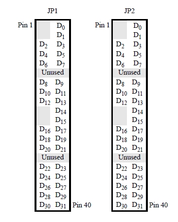
The image below shows where on the 40-pin expansion ports you can find the 32 pins for JP1 and JP2.
.equ ADDR_JP1PORT, 0xFF200060
.equ ADDR_JP1PORT_DIR, 0xFF200064

  movia r2,ADDR_JP1PORT_DIR
  movia r3,0xffffffff
  stwio r3,0(r2)  # Set direction of all 32-bits to output

  movia r2,ADDR_JP1PORT
  movi  r3,0xab
  stwio r3,(r2)   # Write value to output pins
.equ ADDR_JP2PORT, 0xFF200070
.equ ADDR_JP2PORT_DIR, 0xFF200074

  movia r2,ADDR_JP2PORT_DIR
  stwio r0,0(r2)  # Set direction of all 32-bits to input

  movia r2,ADDR_JP2PORT
  ldwio r3,(r2)   # Read value from pins
.equ ADDR_JP1PORT, 0xFF200060
.equ ADDR_JP1PORT_DIR, 0xFF200064
.equ ADDR_JP1PORT_IE, 0xFF200068
.equ ADDR_JP1PORT_EDGE, 0xFF20006C
.equ IRQ_JP1PA, 0x00000800

  movia r2,ADDR_JP1PORT_DIR
  stwio r0,0(r2)  # Set all 32-bits to inputs

  movia r2,ADDR_JP1PORT_IE
  movi  r3,0xf
  stwio r3,0(r2)  # Enable interrupts on 4 LSB pins

  movia r2,IRQ_JP1PA
  wrctl ctl3,r2   # Enable bit 11 - button interrupts on Nios II

  movia r2,1
  wrctl ctl0,r2   # Enable global Interrupts on Nios II
.section .exceptions, "ax"
IHANDLER:
  rdctl et, ctl4          # Check if an external interrupt has occurred
  beq et, r0, SKIP_EA_DEC

  movia r7,IRQ_JP1PA        # test for bit 7 interrupt
  and   r7,et,r7
  beq   r7,r0,EXIT_IHANDLER # if not, exit handler

  movia r2,ADDR_JP1PORT
  ldwio r3,0(r2)  # Read port A data

  /*** Do whatever you want with the data from the pins ***/

  movia r7,ADDR_JP1PORT_EDGE
  stwio r0, 0(r7) # De-assert interrupt - write to edge capture reg


EXIT_IHANDLER:
  subi ea,ea,4    # Replay interrupted instruction for hw interrupts
SKIP_EA_DEC:
  eret
#define ADDR_JP1PORT ((volatile char *) 0xFF200060)
#define ADDR_JP2PORT ((volatile char *) 0xFF200070)
int main()
{
   // init interface directions
   *(ADDR_JP2PORT+4) = 0; //set every JP2 bit direction to input
   *(ADDR_JP1PORT+4) = 0xffffffff; //set every JP1 bit dir to output

   while (1)
   {
      *ADDR_JP1PORT = *ADDR_JP2PORT;
   }
}